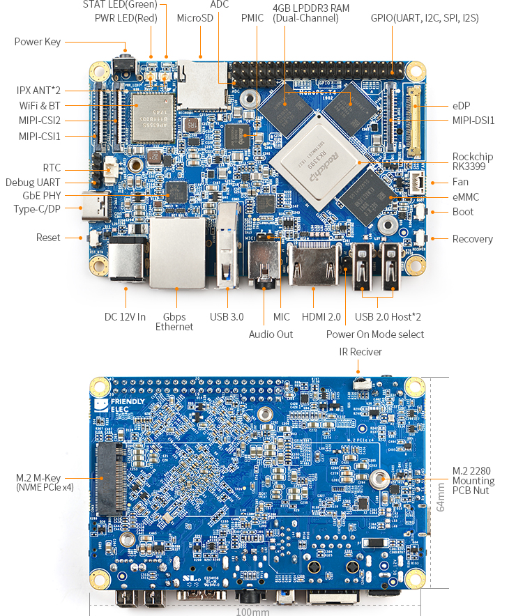
接口布局和尺寸
编辑教程接口布局和尺寸
接口布局
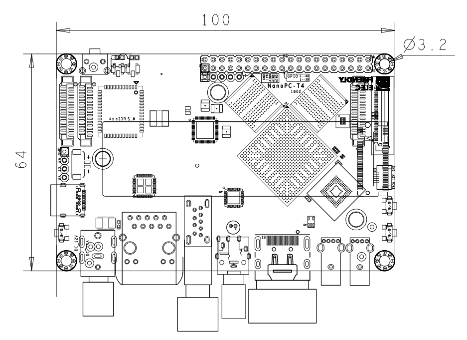
NanoPC-T4 Layout
40 Pin GPIO引脚定义
| Pin# | Assignment | Pin# | Assignment |
|---|---|---|---|
| 1 | VCC3V3_SYS | 2 | VCC5V0_SYS |
| 3 | I2C2_SDA(3V) | 4 | VCC5V0_SYS |
| 5 | I2C2_SCL(3V) | 6 | GND |
| 7 | GPIO1_A0(3V) | 8 | GPIO4_C1/I2C3_SCL(3V) |
| 9 | GND | 10 | GPIO4_C0/I2C3_SDA(3V) |
| 11 | GPIO1_A1(3V) | 12 | GPIO1_C2(3V) |
| 13 | GPIO1_A3(3V) | 14 | GND |
| 15 | GPIO1_A4(3V) | 16 | GPIO1_C6(3V) |
| 17 | VCC3V3_SYS | 18 | GPIO1_C7(3V) |
| 19 | SPI1_TXD/UART4_TX(3V) | 20 | GND |
| 21 | SPI1_RXD/UART4_RX(3V) | 22 | GPIO1_D0(3V) |
| 23 | SPI1_CLK(3V) | 24 | SPI1_CSn0(3V) |
| 25 | GND | 26 | GPIO4_C5/SPDIF_TX(3V) |
| 27 | I2C2_SDA(1.8V) | 28 | I2C2_SCL(1.8V) |
| 29 | I2S1_LRCK_RX(1.8V) | 30 | GND |
| 31 | I2S1_LRCK_TX(1.8V) | 32 | I2S_CLK(1.8V) |
| 33 | I2S1_SCLK(1.8V) | 34 | GND |
| 35 | I2S1_SDI0(1.8V) | 36 | I2S1_SDO0(1.8V) |
| 37 | GPIO3_D4(1.8V) | 38 | GPIO3_D5(1.8V) |
| 39 | GND | 40 | GPIO3_D6(1.8V) |
eDP接口引脚定义
连接器型号: I-PEX-20455-030E
| Pin# | Assignment | Description |
|---|---|---|
| 1 | GND | Signal ground |
| 2 | EDP_TX3N | eDP data lane 3 negative output |
| 3 | EDP_TX3P | eDP data lane 3 positive output |
| 4 | GND | Signal ground |
| 5 | EDP_TX2N | eDP data lane 2 negative output |
| 6 | EDP_TX2P | eDP data lane 2 positive output |
| 7 | GND | Signal ground |
| 8 | EDP_TX1N | eDP data lane 1 negative output |
| 9 | EDP_TX1P | eDP data lane 1 positive output |
| 10 | GND | Signal ground |
| 11 | EDP_TX0N | eDP data lane 0 negative output |
| 12 | EDP_TX0P | eDP data lane 0 positive output |
| 13 | GND | Signal ground |
| 14 | EDPAUXP | eDP CH-AUX positive differential output |
| 15 | EDPAUXN | eDP CH-AUX negative differential output |
| 16 | GND | Signal ground |
| 17 | VCC3V3_SYS | 3.3V Power output for logic |
| 18 | VCC3V3_SYS | 3.3V Power output for logic |
| 19 | I2C4_SDA | 3V I2C data signal, Connect to touch panel |
| 20 | I2C4_SCL | 3V I2C clock signal, Connect to touch panel |
| 21 | GPIO1_C4_TP_INT | 3V interrupt input, Connect to the interrupt output of touch panel |
| 22 | GPIO1_B5_TP_RST | 3V output for reseting touch panel, Connect to the reset input of touch panel |
| 23 | PWM0_BL | 3V PWM output, for LCD backlight dimming. pulled up to VCC3V3_SYS on LCD side. |
| 24 | GPIO4_D5_LCD_BL_EN | 3V output for turning on/off the LCD backlight |
| 25 | GND | Backlight ground |
| 26 | GND | Backlight ground |
| 27 | GND | Backlight ground |
| 28 | VCC12V0_SYS | 12V Power output for Backlight Power |
| 29 | VCC12V0_SYS | 12V Power output for Backlight Power |
| 30 | VCC12V0_SYS | 12V Power output for Backlight Power |
MIPI-DSI接口引脚定义
0.5mm FPC 连接器
| Pin# | Assignment | Description |
|---|---|---|
| 1, 2, 3 | VCC5V0_SYS | 5V power output |
| 4 | GND | Return current path |
| 5 | I2C4_SDA | 3V I2C data signal, Connect to touch panel |
| 6 | I2C4_SCL | 3V I2C clock signal, Connect to touch panel |
| 7 | GND | Return current path |
| 8 | GPIO1_C4_TP_INT | 3V interrupt input, Connect to the interrupt output of touch panel |
| 9 | GND | Return current path |
| 10 | PWM0_BL | 3V PWM output, for LCD backlight dimming |
| 11 | GND | Return current path |
| 12 | GPIO4_D5_LCD_BL_EN | 3V output for turning on/off the LCD backlight |
| 13 | GPIO4_D6_LCD_RST_H | 3V output for reseting the LCD module |
| 14 | GPIO1_B5_TP_RST | 3V output for reseting touch panel, Connect to the reset input of touch panel |
| 15 | GND | Return current path |
| 16 | MIPI_TX0_D3N | MIPI DSI negative differential data line transceiver output |
| 17 | MIPI_TX0_D3P | MIPI DSI positive differential data line transceiver output |
| 18 | GND | Return current path |
| 19 | MIPI_TX0_D2N | MIPI DSI negative differential data line transceiver output |
| 20 | MIPI_TX0_D2P | MIPI DSI positive differential data line transceiver output |
| 21 | GND | Return current path |
| 22 | MIPI_TX0_D1N | MIPI DSI negative differential data line transceiver output |
| 23 | MIPI_TX0_D1P | MIPI DSI positive differential data line transceiver output |
| 24 | GND | Return current path |
| 25 | MIPI_TX0_D0N | MIPI DSI negative differential data line transceiver output |
| 26 | MIPI_TX0_D0P | MIPI DSI positive differential data line transceiver output |
| 27 | GND | Return current path |
| 28 | MIPI_TX0_CLKN | MIPI DSI negative differential clock line transceiver output |
| 29 | MIPI_TX0_CLKP | MIPI DSI positive differential clock line transceiver output |
| 30 | GND | Return current path |
MIPI-CSI接口引脚定义
0.5mm FPC 连接器
MIPI-CSI2也可作为MIPI-DSI接口连接LCD显示屏
| Pin# | MIPI-CSI1 | MIPI-CSI2 | Description |
|---|---|---|---|
| 1 | VCC5V0_SYS | VCC5V0_SYS | 5V Power ouput |
| 2 | VCC5V0_SYS | VCC5V0_SYS | 5V Power ouput |
| 3 | GND | GND | Return current path |
| 4 | VCC_CSI_AF2.8V | VCC_CSI_AF2.8V | 2.8V Power for VCM |
| 5 | VCC_CSI_1.2V | VCC_CSI_1.2V | 1.2V Power for image sensor core circuit |
| 6 | VCC1V8_CAM | VCC1V8_CAM | 1.8V power for I/O circuit |
| 7 | VCC_CSI_2.8V | VCC_CSI_2.8V | 2.8V power for image sensor analog circuit |
| 8 | VCC_CSI_1.0V | VCC_CSI_1.0V | 1.0V Power for image sensor core circuit |
| 9 | I2C1_SCL | I2C2_SCL | 1.8V I2C clock signal |
| 10 | I2C1_SDA | I2C2_SDA | 1.8V I2C data signal |
| 11 | MIPI_CSI0_RST | MIPI_CSI1_RST | reset camera module |
| 12 | MIPI_CSI0_PWN | MIPI_CSI1_PWN | Power down camera module |
| 13 | GND | GND | Return current path |
| 14 | GPIO2_B3_CIF_CLKOUTA | GPIO2_B3_CIF_CLKOUTA | MCLK to camera module |
| 15 | GND | GND | Return current path |
| 16 | MIPI_RX0_D3P | MIPI_TX1/RX1_D3P | MIPI CSI positive differential data line transceiver output |
| 17 | MIPI_RX0_D3N | MIPI_TX1/RX1_D3N | MIPI CSI negative differential data line transceiver output |
| 18 | GND | GND | Return current path |
| 19 | MIPI_RX0_D2P | MIPI_TX1/RX1_D2P | MIPI CSI positive differential data line transceiver output |
| 20 | MIPI_RX0_D2N | MIPI_TX1/RX1_D2N | MIPI CSI negative differential data line transceiver output |
| 21 | GND | GND | Return current path |
| 22 | MIPI_RX0_D1P | MIPI_TX1/RX1_D1P | MIPI CSI positive differential data line transceiver output |
| 23 | MIPI_RX0_D1N | MIPI_TX1/RX1_D1N | MIPI CSI negative differential data line transceiver output |
| 24 | GND | GND | Return current path |
| 25 | MIPI_RX0_CLKP | MIPI_TX1/RX1_CLKP | MIPI CSI positive differential clock line transceiver output |
| 26 | MIPI_RX0_CLKN | MIPI_TX1/RX1_CLKN | MIPI CSI negative differential clock line transceiver output |
| 27 | GND | GND | Return current path |
| 28 | MIPI_RX0_D0P | MIPI_TX1/RX1_D0P | MIPI CSI positive differential data line transceiver output |
| 29 | MIPI_RX0_D0N | MIPI_TX1/RX1_D0N | MIPI CSI negative differential data line transceiver output |
| 30 | GND | GND | Return current path |
M.2 PCIe接口引脚定义
PCIe Gen 2.1 x4
M.2 Key M Connector for Socket 2/Socket 3 PCIe-based Module, such as PCIe SSD
连接器型号: MDT-420-M-01002
| Pin# | Assignment | Description | Pin# | Assignment | Description |
|---|---|---|---|---|---|
| 1 | GND | Return current path | 2 | VCC3V3_SYS | 3.3V Power output |
| 3 | GND | Return current path | 4 | VCC3V3_SYS | 3.3V Power output |
| 5 | PCIE_RX3_N | PCIe differential data input signals | 6 | N/C | no connection |
| 7 | PCIE_RX3_P | PCIe differential data input signals | 8 | N/C | no connection |
| 9 | GND | Return current path | 10 | N/C | no connection |
| 11 | PCIE_TX3N | PCIe differential data output signals | 12 | VCC3V3_SYS | 3.3V Power output |
| 13 | PCIE_TX3P | PCIe differential data output signals | 14 | VCC3V3_SYS | 3.3V Power output |
| 15 | GND | Return current path | 16 | VCC3V3_SYS | 3.3V Power output |
| 17 | PCIE_RX2_N | PCIe differential data input signals | 18 | VCC3V3_SYS | 3.3V Power output |
| 19 | PCIE_RX2_P | PCIe differential data input signals | 20 | N/C | no connection |
| 21 | GND | Return current path | 22 | N/C | no connection |
| 23 | PCIE_TX2N | PCIe differential data output signals | 24 | N/C | no connection |
| 25 | PCIE_TX2P | PCIe differential data output signals | 26 | N/C | no connection |
| 27 | GND | Return current path | 28 | N/C | no connection |
| 29 | PCIE_RX1_N | PCIe differential data input signals | 30 | N/C | no connection |
| 31 | PCIE_RX1_P | PCIe differential data input signals | 32 | N/C | no connection |
| 33 | GND | Return current path | 34 | N/C | no connection |
| 35 | PCIE_TX1N | PCIe differential data output signals | 36 | N/C | no connection |
| 37 | PCIE_TX1P | PCIe differential data output signals | 38 | DEVSLP/NC | internal pull up to VCC3V3_SYS with 10K |
| 39 | GND | Return current path | 40 | I2C2_SCL | 1.8V I2C clock signal |
| 41 | PCIE_RX0_N | PCIe differential data input signals | 42 | I2C2_SDA | 1.8V I2C data signal |
| 43 | PCIE_RX0_P | PCIe differential data input signals | 44 | GPIO2_A2_PCIE_ALERT# | 1.8V GPIO signal |
| 45 | GND | Return current path | 46 | N/C | no connection |
| 47 | PCIE_TX0N | PCIe differential data output signals | 48 | N/C | no connection |
| 49 | PCIE_TX0P | PCIe differential data output signals | 50 | GPIO2_A4_PCIE_RESET# | 1.8V GPIO signal |
| 51 | GND | Return current path | 52 | CLKREQ#/NC | internal pull down to GND with 0R |
| 53 | PCIE_REF_CLKN | differential reference clock out for PCIe peripheral | 54 | GPIO2_A3_PCIE_WAKE# | 1.8V GPIO signal |
| 55 | PCIE_REF_CLKP | differential reference clock out for PCIe peripheral | 56 | N/C | no connection |
| 57 | GND | Return current path | 58 | N/C | no connection |
| 59 | Connector Key | Connector Key | 60 | Connector Key | Connector Key |
| 60 | Connector Key | Connector Key | 61 | Connector Key | Connector Key |
| 62 | Connector Key | Connector Key | 63 | Connector Key | Connector Key |
| 64 | Connector Key | Connector Key | 65 | Connector Key | Connector Key |
| 66 | Connector Key | Connector Key | 67 | N/C | no connection |
| 68 | RTC_CLKO_SOC | 1.8V 32.768KHz clock output | 69 | N/C | no connection |
| 70 | VCC3V3_SYS | 3.3V Power output | 71 | GND | Return current path |
| 72 | VCC3V3_SYS | 3.3V Power output | 73 | GND | Return current path |
| 74 | VCC3V3_SYS | 3.3V Power output | 75 | GND | Return current path |
ADC接口引脚定义
ADC输入范围 : 0~1.8V
| Pin# | Assignment |
|---|---|
| 1 | GND |
| 2 | VCC_1V8 |
| 3 | ADC_IN0 |
| 4 | ADC_IN2 |
| 5 | ADC_IN3 |
散热风扇接口引脚定义
连接器型号: JST GH系列连接器,3Pin,BM03B-GHS-TBT
| Pin# | Assignment Description |
|---|---|
| 1 | GND 0V |
| 2 | 12V 12V output ,controlled by GPIO4_C6/PWM1 |
| 3 | GPIO2_A6_FAN_TACH connect to tachometer output signal , or float |
调试串口引脚定义
3V电平, 波特率1500000bps
| Pin# | Assignment | Description |
|---|---|---|
| 1 | GND | 0V |
| 2 | VCC5V0_SYS | 5V power output |
| 3 | UART2DBG_TX | output |
| 4 | UART2DBG_RX | intput |
电源接口
DC-12V/2A输入, 5.5*2.1mm DC电源接口
电源按键
板子处于关机状态时,需要按下电源按键(大于0.5秒,PWR灯亮即可松开)才会开机.
当板子已正常启动,则电源按键的功能与系统有关,例如在安卓系统下,短按进入休眠,或唤醒,长按则显示关机/重启界面.
USB接口
- USB Type-C 接口具有2A过流保护功能.
- USB 3.0 接口具有2A过流保护功能.
两个USB 2.0接口共享2A过流保护, 也就是说2个接口的负载总和不应超过2A, 否则触发保护, 2个接口上的设备都会被切断电源.
BOOT按键
按下BOOT按键可以阻止板子从eMMC启动系统; 当板子无法从eMMC和tf卡启动系统时, 板子就会进入MASKROM模式; MASKROM模式下, 可以通过Type-C接口更新板子的系统.
RTC
- 我们实测的RTC备份电流为27uA.
- 连接器型号: Molex 53398-0271
其他说明
- 只能从DC电源接口给板子供电, 其他接口的电源引脚均为输出引脚.
- 修改板子为上电即开机的方法(改后不再保修)
- 原理图: 板子原理图
尺寸
Mos固件,小电视必刷固件
ES6 教程
Vue.js 教程
JSON 教程
jQuery 教程
HTML 教程
HTML 5 教程
CSS 教程
CSS3 教程
JavaScript 教程
DHTML 教程
JSON在线格式化工具
JS在线运行
JSON解析格式化
jsfiddle中国国内版本
JS代码在线运行
PHP代码在线运行
Java代码在线运行
C语言代码在线运行
C++代码在线运行
Python代码在线运行
Go语言代码在线运行
C#代码在线运行
JSRUN闪电教程系统是国内最先开创的教程维护系统, 所有工程师都可以参与共同维护的闪电教程,让知识的积累变得统一完整、自成体系。
大家可以一起参与进共编,让零散的知识点帮助更多的人。
X

选择支付方式:


立即支付
¥
9.99
无法付款,请点击这里
金额: 0 元
备注:
转账时请填写正确的金额和备注信息,到账由人工处理,可能需要较长时间
备注:
转账时请填写正确的金额和备注信息,到账由人工处理,可能需要较长时间
如有疑问请联系QQ:565830900
正在生成二维码, 此过程可能需要15秒钟